
introduces,
A Prototyped & Patented Clean Breakthrough
Technology Process
In The High Demand Semiconductor Manufacturing Industry
PATENTED: No. 10-1436553/Korea for a "new method of manufacturing semiconductor device & equipment for through-silicon-via structure".
US NOTICE OF ALLOWANCE ISSUED JUNE 21':
US PATENT No. 16-750,909 for a "new method of manufacturing semiconductor device & equipment for through-silicon-via structure".
PCT APPLICATION FILED 2021:
For a "new method of manufacturing semiconductor device & equipment for through-silicon-via structure".
NEXT LEVEL SEMICONDUCTOR TECHNOLOGY PROCESS BREAKTHROUGH
introduces,
A Patented Clean Breakthrough Technology Process
In The High Demand Semiconductor Manufacturing Industry
PATENTED: No. 10-1436553/Korea for a "new method of manufacturing semiconductor device & equipment for through-silicon-via structure".
US NOTICE OF ALLOWANCE ISSUED JUNE 21':
US PATENT No. 16-750,909 for a "new method of manufacturing semiconductor device & equipment for through-silicon-via structure".
PCT APPLICATION FILED 2021:
For a "new method of manufacturing semiconductor device & equipment for through-silicon-via structure".
The US Senate has passed the Biden's administrations ambitious CHIPS programs.
The CHIPS For America Act aims to support domestic USA semiconductor manufacturing during the global shortage and various challenges facing conventional manufacturing techniques, such as pollution, further miniaturization and multiple functions layering, which are overcome by the TFI breakthrough patented process.
This new 3DIC (three-dimensional integrated circuit) is an exceptionally innovative development that can overcome the communication bottleneck of 2D—moving data between chips—through the dense and fine-grain integration of computating and data storage. This will allow massive data storage and faster processing to convert data into useful information. TFI’s new process—what is called the wet metallization process— for the 3DIC is more sustainable than any semiconductor manufacturing process available today.
TFI is more efficient, green, and allows more layering of multifunction, more miniaturization, plus customization, and yields a remarkable 40% reduction in chip process costs, affording lower consumer prices for devices – and more profitability to companies, while helping to protect the environment.
TFI was established in 2018 and in 2020 TFI USA established a worldwide exclusive, perpetual Licensing Agreement with TFI South Korea for all Assets, R&D, the functional Prototype, Intellectual Property, etc.
TFI USA is now a part of the California Manufacturers Council that helps tech manufacturing companies.
TFI has secured the US Patent and Trademark Office allowance of the powerful USA Utility Patent and has begun the Patent Cooperation Treaty (PCT) international applications.
TFI is currently planning to relocate the demo lab to Irvine, Orange County, California and raising funding for tool manufacturing and major customer demos.
TFI's new process 3D technology has the potential to be the platform for many revolutionary applications in the future without compromising the environmental welfare.
TFIS OFFERS A REVOLUTIONARY SEMICONDUCTOR MANUFACTURING PROCESS
"Taiwan Semiconductor Manufacturing, the Worlds Largest Chip Manufacturer, is Raising Prices As Much As 20%."
- reportlinker.com from the Wall Street Journal 2021
“We are at the doorstep of the largest shift in the semiconductor industry ever, one that will
dwarf the PC and even the consumer electronics eras (..) all based on 3D silicon technology”
Dr. Chang-Gyu Hwang, President & CEO, Samsung Semiconductor, IEDM Conference
“We are at the doorstep of the largest shift in the semiconductor industry ever, one that will
dwarf the PC and even the consumer electronics eras (..) all based on 3D silicon technology”
Dr. Chang-Gyu Hwang, President & CEO, Samsung Semiconductor, IEDM Conference
TFIS OFFERS A REVOLUTIONARY SEMICONDUCTOR MANUFACTURING PROCESS
"Taiwan Semiconductor Manufacturing, the Worlds Largest Chip Manufacturer, is Raising Prices As Much As 20%."
- reportlinker.com from the Wall Street Journal 2021
See TFIS' latest investor news!
ADVANCEDCHIPS Bulletin released Spring 2023!
See TFIS' latest investor news!
ADVANCEDCHIPS Bulletin released August 2021
TFIS' new process and proprietary equipment overcomes major issues and problems of current PVD, sputtering process and equipment limitations.
The demand For semiconductors is ever growing into new vital industries, such as contactless solutions, including touch screens and elevator buttons, ambient assisted-living devices, including sensors, that help elderly and chronically ill patients remain in their homes, rather than moving to facilities, automated-delivery solutions for the last mile, such as robots and drones, and includes use in all current electronic devices.
PROBLEM
TFI Solves The Limitations & Negative Impacts of Conventional Manufacturing for Semiconductor 'CHIP's
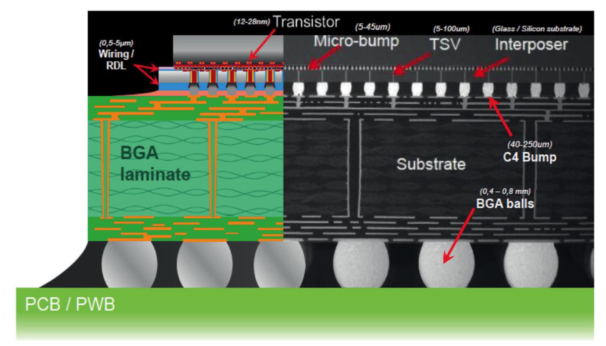
TSV application for Wide I/O memory details
The TSV process performance of 3DIC to be affected by metal (conductor & barrier) capability but poor Step Coverage of Copper layer related made it worse and PVD CoO is really high for now.
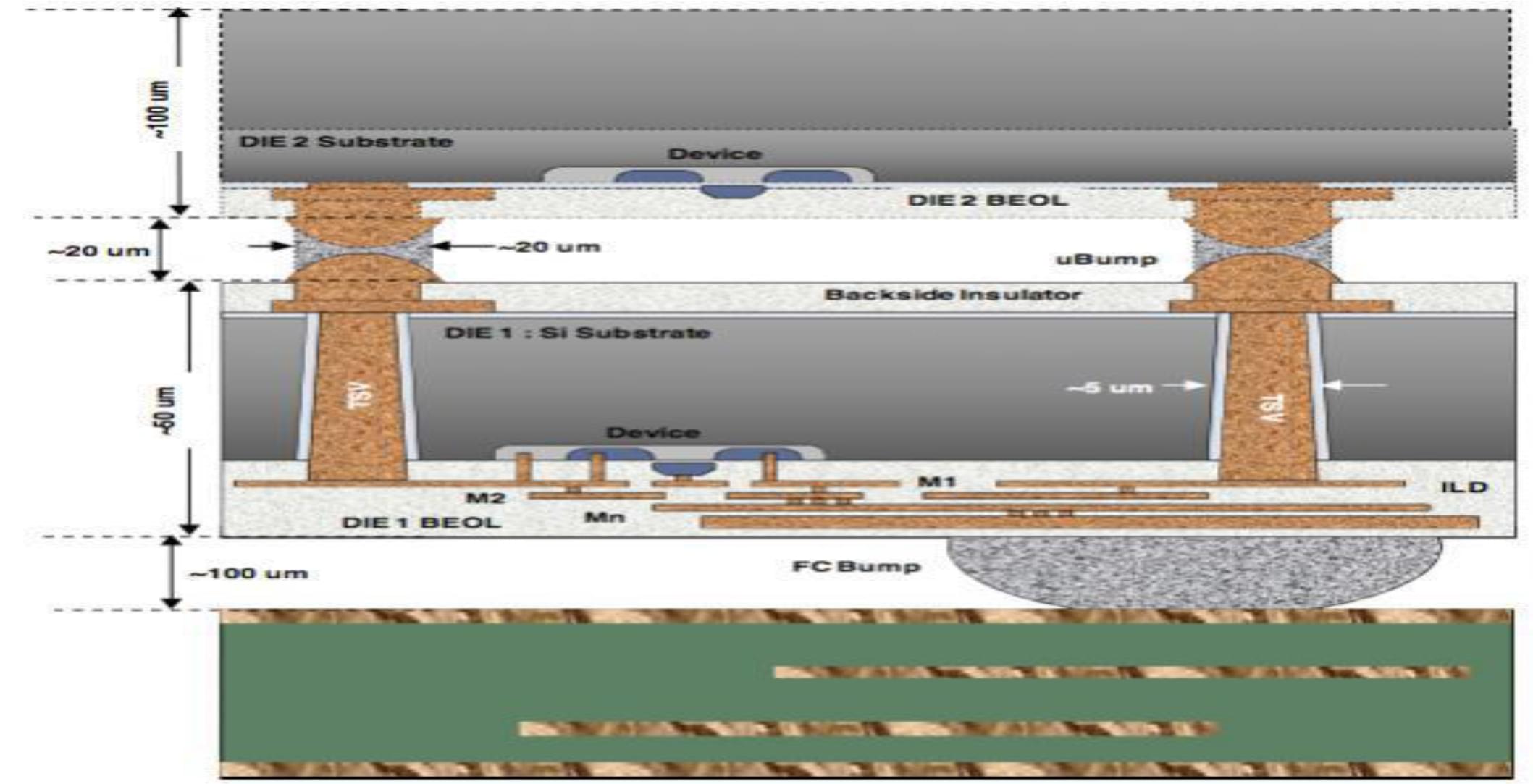
Poor Step Coverage (now less than 5% by PVD required more than 50%), low throughput, high CoO (Cost of Ownership)
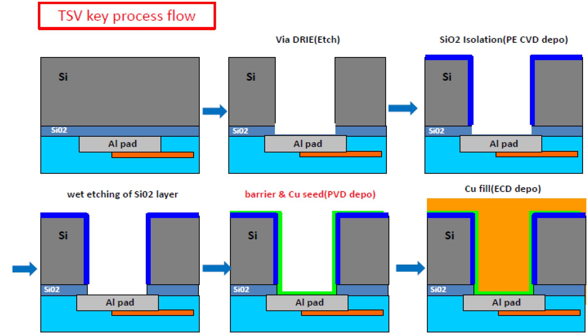
TSV Dry Process Limitations,
Demand a Different Approach
So PVD came to process limitation and market required new solutions to deposit metal in TSV device of 3DIC.
TFI’s new process and proprietary equipment overcomes major issues and problems of current PVD, sputtering process and equipment limitations.
Time for TSV 3D is Now!
SOLUTION
NEW ALL WET METAL PROCESS

New Deposition Technology
- Better step coverage: over 50%
- Available for High Aspect Ratio : > 10:1
- Conformal metal layer deposition and stability
- Low Capex, high efficiency, reasonable CoO
-
Provide in-cluster tool for wet metal process
NEXT LEVEL SEMICONDUCTOR TECHNOLOGY PROCESS BREAKTHROUGH
Intel's new ceo has said there could be a global shortage of semiconductors for several years according to a reuters report.
This will affect consumer electronics such as computers, smartphones, and tablets to the point
where consumers could see prices increase.
THE TFIS USA COMPANY
Ty (Tae Young)
Lee
FOUNDER, PRESIDENT & CHAIRMAN OF THE BOARD

Prof. Alan Tratner
Co-CEO

Winston(Wan Soo), Ra
VP, SALES & MARKETING
YT(Youn Tak), Park
COO & BOARD
Terry Collins
COO & Advisory Board
- Experienced Technology management and consulting.
- Diverse leadership experience from marquis companies including: Computer Associates and Cognos to start-ups.
- Proven ability to develop and execute strategic plans to achieve objectives.
- Balanced experience in complex multi-member technology delivery teams.
- Insightful communication and presentation skills from executives to staff level consultants.
- Direct management responsibility for P&L’s ranging from 8 to 65 resources.
- Oversight and management of multiple simultaneous project teams.
- International experience establishing a sales/consulting office in Saudi Arabia.
Kathie Callahan Brady
Executive Business Advisory Board
Kathie Callahan Brady works with some highly gifted, emerging Biotech and Technology companies as President and CEO of Frederick Innovative Technology Center, Inc. (FITCI). Since stepping into her role at the incubator/ accelerator in 2016, FITCI has seen its client base grow 476%. Currently, they serve 72 companies, and in total have served over 200+ companies. She herself is an entrepreneur with more than 30 years of executive-level experience in IT, real estate, and business development. She’s led entrepreneurs and corporations in strategies to achieve high-level success. Kathie has founded and helped grow four successful companies in various industries including real estate, telecommunications, healthy lifestyles (Naturopathic Medicine), and consulting.
Join the Rare Opportunity to Invest in a High Demand, Clean & High Tech USA CHIP Company
With valuable IP secured in S. Korea, allowable in the USA, and filed for international rights, TFIS and its vital breakthrough technology has made an offering on the Title III Crowdfunding to accredited and non-accredited investors for a limited time.
Investments in private companies and securities are speculative, generally illiquid, and are particularly risky and may result in total loss of invested capital. The past performance of a security or a company does not guarantee future results or returns. Only investors who understand the risks of early-stage investment and who meet the investment criteria outlined by Title3Funds.com may invest.
USA Headquarters
1176 Tourmaline Dr.
Thousand Oaks, CA 93065
Tel.+82-10-5473-5171
tfi@tfitec.com
South Korea Headquarters
#408, Daewoo Frontier Valley 1
1030 Jung-dong, Giheung, Yongin,
Gyeonggi-do, South Korea 17015
Tel.010-5473-5171 tylee@tfitec.com
All Rights Reserved.